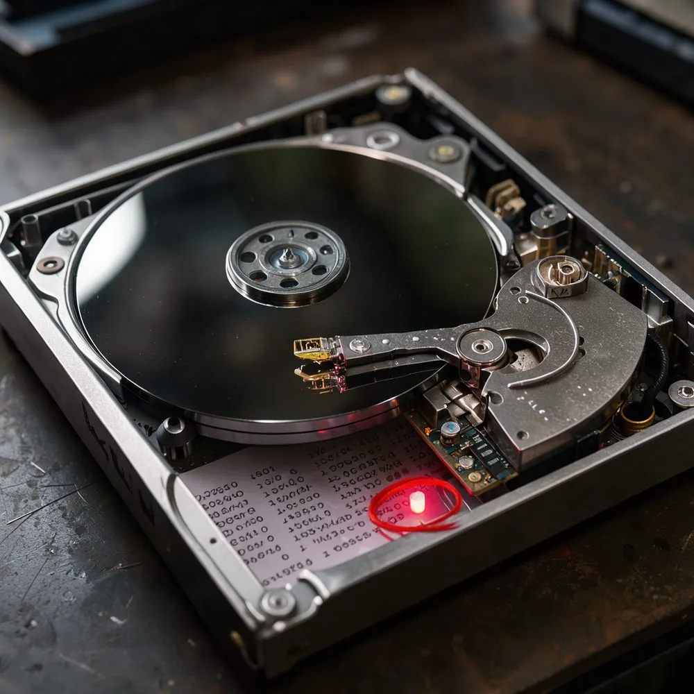
AMD's new AI GPU holds 288GB of memory, built from eight 36GB stacks
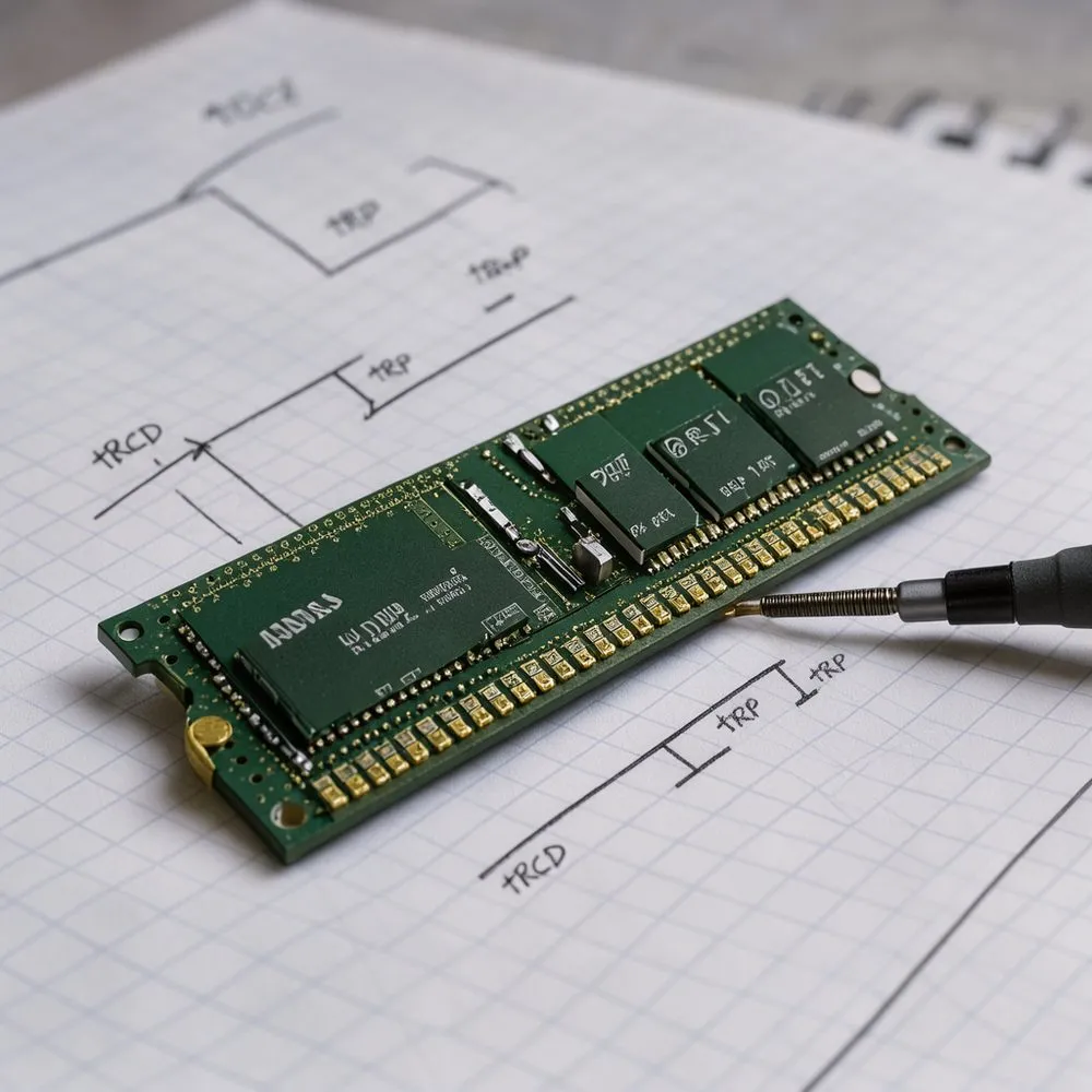
The most useful number in AMD's new AI GPU announcement is not 288 gigabytes. It is 36. Semiconductor Engineering's November 13 week-in-review mentions the card in a single line, "an AI GPU with 288GB of HBM4," with no stack count, no bandwidth and no clock (semiengineering.com/chip-industry-week-in-revie…). That is enough to do the arithmetic a packaging engineer would do first.
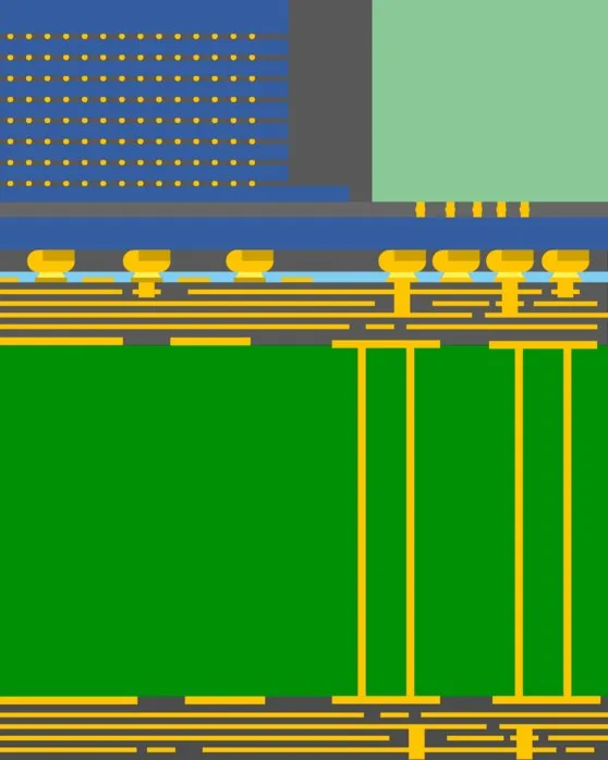
HBM, high bandwidth memory, is DRAM built as a vertical tower instead of a flat stick. Each die in the tower is drilled and wired edge to edge with TSVs, through-silicon vias, which are vertical copper connections, and the finished towers sit on the same package as the processor, on a silicon interposer that acts as the wiring substrate between them. A stack is one of those towers. If each HBM4 stack holds 36GB, then 288 divided by 36 is exactly 8 stacks. A 36GB tower would be twelve 3GB dies stacked and wired, if that is how the dies are divided. So 288GB is a standard-shaped package, not a density surprise.
Capacity and bandwidth are separate curves. Capacity per package is stacks times dies per stack times die density. Bandwidth per package is stacks times interface width times clock. Taller stacks and denser dies buy gigabytes. More stacks or wider interfaces buy gigabytes per second. Both are bounded by how much silicon and how many wires fit on the interposer under the heat spreader. That wire count, and the interposer area it needs, is one ceiling on the package.
The same issue carries a useful comparison from the other end of the industry. Infineon reported fabricating functional power devices on 300mm silicon carbide wafers at its Villach, Austria fab using existing silicon processing equipment, with each wafer holding 2.3 times as many chips as a 200mm one. That is a manufacturing cost argument, the same kind of arithmetic as the HBM stack count: a change in the number of units per carrier, not a change in what each unit does. Imec also completed baseline process flows for its NanoIC silicon-interposer platform, with a PDK planned for early 2027.
What the 288GB figure does not tell you is the shipped configuration. Eight stacks of 36GB is my division until AMD publishes the stack count and bandwidth. The open questions are whether the stacks are 12-high with 3GB dies or some other division, and what per-stack bandwidth AMD claims. A product slide would settle the stack count, the interface width and the clock. The roundup gives none of them, and a capacity number without those three is a packaging decision waiting for its datasheet.