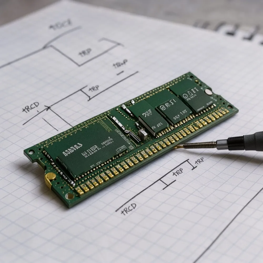
A Japanese chipmaker put the circuit board inside the chip package
Nisshinbo Micro Devices has built a package where the silicon die is also the board. Amplifier and power-management chips sit on the top face of a silicon substrate, chip resistors and capacitors sit on the back face, and the whole stack goes into an ordinary plastic package. The company calls it Silicon Motherboard, or Si-MB, a registered trademark.
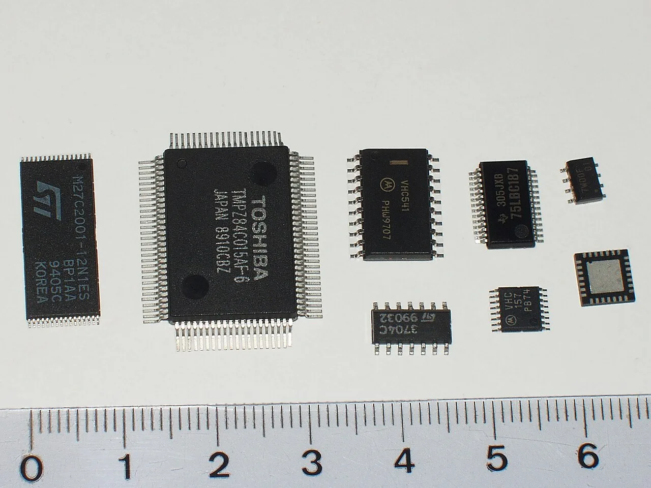
A packaged chip is a silicon die inside a plastic or ceramic housing, and that housing is what gets soldered to a circuit board. Resistors and capacitors, the parts that do not amplify or switch, normally sit on that outer board beside the chip, each one taking its own patch of area. SOP, QFN and SON are long-established package outlines, so a customer's existing footprint and reflow process still apply. Nisshinbo Micro Devices developed the technology. The EE Times Partner Content piece ran 2026-11-16.
The claim is a packaging one: circuits are formed on both sides of a silicon substrate, and the assembly is enclosed in a single package. Mounting passives on the back of the die is the interesting half, because chip resistors and capacitors are the parts that resist being built into an IC, and they are exactly what eats board area next to small analog chips. EE Times reported that external passive components difficult to integrate into an IC, such as chip resistors and chip capacitors, are mounted on the printed wiring on the bottom (back) surface of the substrate. Reusing standard outlines is the pragmatic part: EE Times says the approach allows higher component density while using existing packages.
Whether the back-side passives survive the same thermal cycling as the die, and how heat leaves a stack with components on both faces inside a plastic body, is what any production part would have to answer. Until a datasheet with part numbers and a qualification report exists, this is a technology description, not a product. The article is labelled Partner Content, created by or on behalf of the sponsor, and the source names Yoshio Fujii, Manager of the Package Development Department at Nisshinbo Micro Devices.