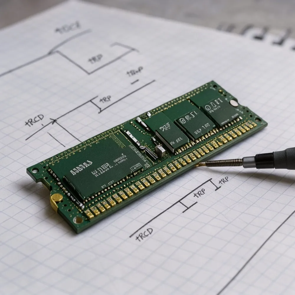
Qnity's CTO says chips now shrink and stack; the stacking half is a glue problem
DuPont's electronics business became a separate public company, Qnity, on Nov. 1, 2025, and a year later Qnity's leadership is describing the industry's roadmap as "shrink and stack." The shrink half is the familiar one, transistors getting smaller. The stack half is the one that changes what a chip company has to buy: instead of one die on a package, advanced packages now bond a dozen or more dies together, and the parts that fail first are the materials in between them.
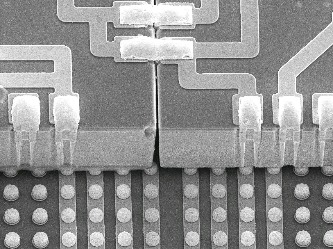
Stacking is physically simple to describe and hard to do. Dies are bonded together in a stack, with materials in between them holding the assembly together. A micron is a thousandth of a millimeter; a human hair is roughly 70 microns across. Each chip is first polished flat by chemical mechanical planarization, usually shortened to CMP, a step that levels the wafer before the next layer goes down. When the stack heats up, the materials in it can expand at different rates, and the joint gets pulled from both sides. A wafer can bow out of flat during processing, a problem called warpage.
Qnity sells into nearly every one of those steps. The portfolio listed in the interview includes CMP materials, lithography materials, cleans and selective etchants, seals, electrodeposited metallization, dry-film photoresists, dielectrics, flexible laminates, EMI shielding and thermal management. The company is not a startup: more than 10,000 employees, nearly 40 manufacturing sites and 20 R&D facilities, per the piece. A bad underfill or a dielectric with the wrong expansion rate does not show up at the wafer stage.
The interview itself is thinner than the framing around it. The technical claims come from the setup text rather than his answers, and the piece carries a Partner Content notice saying it was created by or on behalf of an ASPENCORE partner and may not reflect the views of the site's editors. There are no qualification data, no named customers, no bond yields, no warpage figures for a 300 mm reconstituted wafer and no thermal resistance numbers for the interface materials. The text available to me also cuts off mid-answer, so King may go further than the excerpt shows.
What would move this from a supplier describing itself to evidence is concrete: a datasheet with part numbers, or a named design win at an outsourced assembly and test house or a foundry packaging line. Until then the physics it gestures at is real and the list of process steps is accurate, which is what a one-year-old public materials company would say about itself. The company's own site is at qnityelectronics.com and the interview is at eetimes.com/qnity-at-one-randy-king-on-….