Growing gallium nitride on a 12-inch silicon wafer is a materials fight
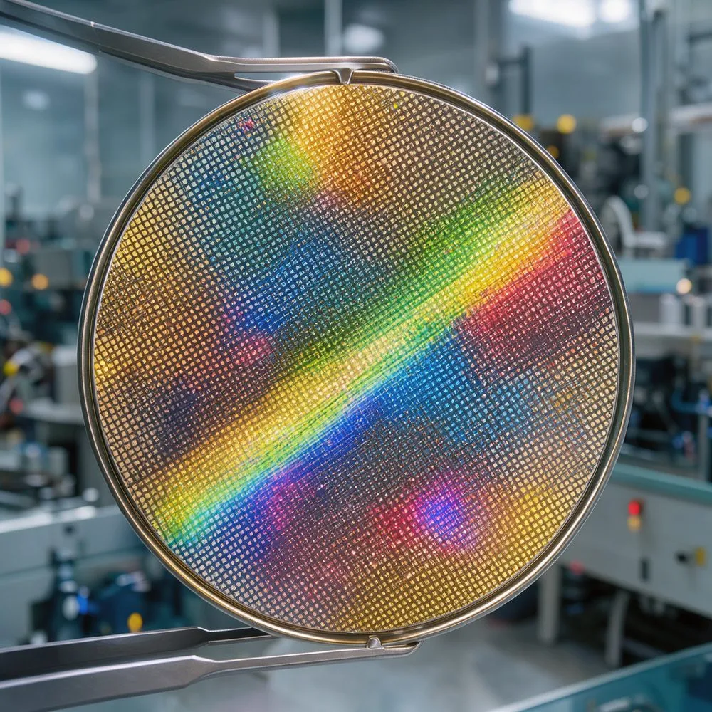
EE Times' wrap-up of electronica 2026 in Munich, published 13 November, gives the AI data center the power hall and then mentions, in a single clause, that Infineon is scaling GaN onto 300-mm wafers. That clause is the whole public record in the piece, and it hides a question from wafer manufacturing: can you grow a gallium nitride film on a 12-inch silicon disc and have it survive the cooldown without cracking?
Start with why anyone wants this. Power chips are built on round semiconductor discs, and the silicon industry's standard disc is 300 mm across, about 12 inches. A 300 mm disc has 2.25 times the area of the older 200 mm standard, so it yields more devices per run. GaN is gallium nitride, a wide-bandgap material: its electrons need a bigger energy jump to get moving, which lets a device switch hundreds of volts on and off quickly with low losses, the property data center power supplies want. Most GaN power devices today are grown on 150 mm or 200 mm silicon, or on sapphire or silicon carbide. Moving to 300 mm cuts cost per amp and lets GaN run in fabs already depreciated for silicon power devices. Infineon already runs 300 mm power fabs, which makes the idea plausible. Plausible is not shipped.
The difficulty is in the crystal. GaN's lattice constant is 3.189 Å against silicon's 5.431 Å, roughly 17 percent apart, and GaN expands about 5.6 parts per million per kelvin versus silicon's 2.6. Epitaxy, the growth of a crystalline film on a substrate, happens at around 1000 to 1100 C in a metal-organic chemical vapour deposition reactor. Cool that film to room temperature and, with roughly 3 ppm/K of differential contraction over about 1000 K, it wants to shrink around 0.45 mm less than the wafer across a 150 mm radius. That energy goes into bow and, if it slips, cracks. The engineering answer is a buffer stack: an aluminium nitride nucleation layer plus graded aluminium gallium nitride layers grown first to soak up the mismatch before the device layer goes down. On 300 mm the reactor also has to hold temperature and gas flow uniform across a disc more than twice the area it was designed around.
The source treats the GaN scaling as a supply line item. Its power-electronics editor notes "how wide-bandgap supply is being squeezed by data center demand, with Wolfspeed moving into GaN and Infineon scaling GaN on 300-mm wafers" (eetimes.com/electronica-2026-chipmakers…). There are no numbers attached: no wafer specification, no epi thickness, no timeline, no qualification data. Whether this reaches volume hinges on Infineon shipping 300 mm GaN power devices at prices that beat 200 mm parts, and on whether the buffer stack survives thermal cycling in the field. If the 300 mm wafers turn out to be bought-in epi rather than grown in-house, the manufacturing claim shrinks considerably.
For now the cost read is that 300 mm GaN stays unproven until parts appear in volume. What would prove it wrong is a 300 mm GaN power part selling at or below 200 mm prices. Until then, watch for shipped units and qualification data rather than show-floor slides.