Google's new AI chip moves data at 17.2 TB/s, about 200 times a laptop's memory

Google has two more AI accelerator systems out this week, and one of them is built around a single number: 17.2 terabytes per second of memory bandwidth. The source does not give a laptop comparison, but it does say this is the spec that decides whether an AI agent reading a whole codebase, or hours of video, feels usable or feels like waiting.
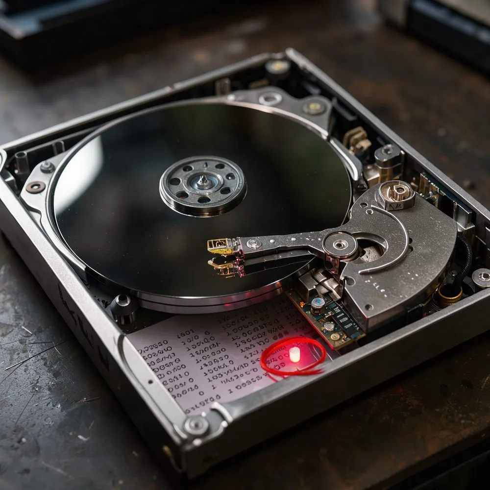
The chip is the TPU 8i Max. It is not a new design: Google took two of its inference-focused TPU 8i chips and put both dies in one physical package. That doubles the compute, doubles the on-chip scratch memory (SRAM, fast memory on the chip itself, to 768 MB) and doubles the HBM bandwidth. HBM is high-bandwidth memory, stacked layers of memory sitting right next to the AI chip where a model's working data lives. Capacity rises less: 384 GB of HBM, about a third more than a single 8i. ServerTheHome puts the reason plainly: "When many agents work across an entire codebase or hours of video simultaneously, memory bandwidth becomes the bottleneck before compute does." A model with a long context window (how much text, code or video it can hold in view at once) spends its time fetching data, not doing arithmetic, so feeding memory faster is what shortens the wait. The source does not say how the doubled bandwidth is divided between the two dies.
The other system, TPU 8tx, is the same silicon as the training-focused TPU 8t, but paired with AMD's 5th Gen EPYC Turin server processors as the host CPU, the ordinary processor that feeds the accelerator. Its purpose is confidential computing: encrypting data while it is being processed, not just while it sits on disk or crosses a network. Normally data has to be unlocked in memory for a computer to work on it. A dual-socket Turin setup gives 128 PCIe Gen5 lanes, enough for four TPUs plus high-speed network cards with no oversubscription, meaning no device waits its turn on the wire. Google noted that a Gen6 host like EPYC Venice would step down to Gen5 speeds without adding accelerator bandwidth, aligning with its 2027 hardware qualification schedule. The 8tx also borrows the Boardfly network from the inference chip: a layout where the furthest two chips are seven hops apart, against sixteen in the training torus. Google claims up to 2x lower latency than TPU 8t with near-zero performance penalty, its own figure, not an independent measurement.
It is the first time Google has introduced four distinct system configurations in a single year, though not four new chip designs. The 8i Max is the one aimed at the memory wall: the source says memory bandwidth becomes the bottleneck before compute does when many agents work across a codebase or hours of video at once. Whether doubling bandwidth halves the wait, or just moves the bottleneck to the network between chips, is not settled. Google has not published measured throughput for long-context agent workloads on the 8i Max, so the case rests on the spec sheet until someone benchmarks it. servethehome.com/google-tpu-8tx-8i-max-amd-e…