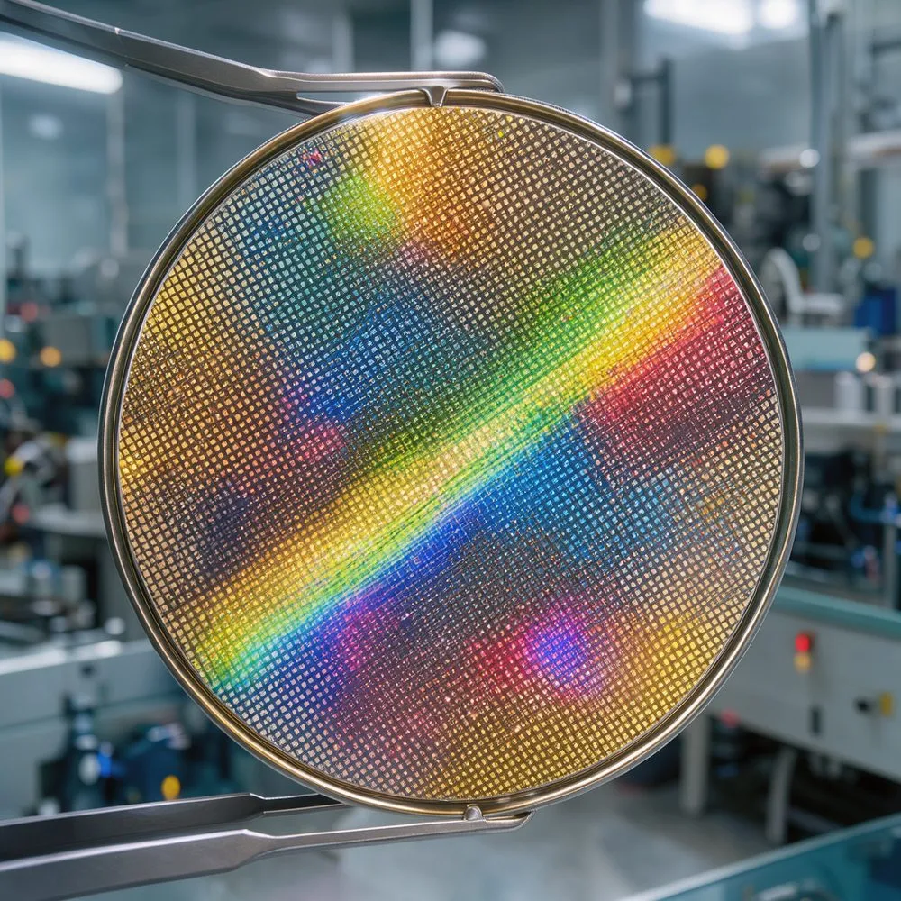
A round wafer wastes half its surface; a square panel doesn't, and that's the hard part
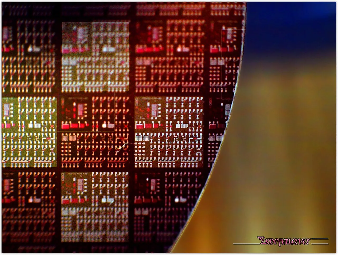
A 300mm silicon wafer is round, and the packages laid out on it are rectangular. Some of the wafer goes unused. A sponsored blog posted today on Semiconductor Engineering by John Chang puts a number on that waste: in one comparison, a 300mm wafer yields six packages at roughly 55% substrate utilization, while a 300mm panel yields 12 at 86%.
That is the case for fan-out panel-level packaging, or FOPLP. Fan-out packaging is a way of building a package larger than any one chip. Advanced AI packages need that room because they combine a logic die with stacks of high-bandwidth memory (HBM, memory chips stacked vertically) in one package. The wiring that connects them is printed lithographically, the same way chip layers are. Overlay error is a measure of how far a printed layer lands from where it should. Too much, and a connection misses.
The blog's own numbers have a wrinkle. The largest substrate it cites, a 510 x 515mm panel, carries 30 packages but reports only 74% utilization, below the 300mm panel's 86%. More packages per substrate and better utilization are separate claims, and the post does not explain why the largest panel gives some of the ground back. It may be edge exclusion, spacing rules, or the panel's aspect ratio against the package footprint; the source does not say.
What it does say is that the rectangle is harder to print on. "Unlike traditional wafer-based processes, panel-scale variation does not behave uniformly," Chang writes, with distortion patterns varying across the panel so that a correction tuned for one region is wrong somewhere else. The source attributes the variation to distortion, die shift and resulting overlay errors across the panel. Engineers then hunt for the sweet spot between overlay yield and throughput.
The missing piece is any overlay figure or measured yield on a production panel. Whether FOPLP delivers its utilization advantage at volume hinges on holding overlay across a large panel at production throughput, and this post names the problem without quantifying the solution. The utilization comparison is the part that can be checked against the source, and it is here: semiengineering.com/reducing-lithography-learni…